Veldhoven, Netherlands, March 2, 2026 — Brussels Morning NewsPaper — that Chipmaking beyond EUV is rapidly becoming the semiconductor industry’s most closely watched frontier as global demand for artificial intelligence hardware accelerates. In 2026, engineers, policymakers, and chip designers are focused on how chipmaking beyond EUV can extend performance gains while addressing the physical limits that traditional extreme ultraviolet lithography now faces.
For years, EUV technology enabled smaller nodes and higher transistor density, sustaining the computing improvements that powered smartphones, cloud services, and data centres. Today, chipmaking beyond EUV represents the next evolution in semiconductor manufacturing, designed to support increasingly complex AI processors and high performance computing systems.
As artificial intelligence transforms industries from finance to healthcare, the tools that manufacture advanced chips have become strategically vital infrastructure. The transition toward chipmaking beyond EUV signals not just technological progress but also economic and geopolitical significance.
The Technical Limits of EUV Lithography
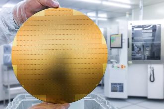
Extreme ultraviolet lithography revolutionized semiconductor production by enabling chipmakers to print incredibly fine circuit patterns. However, the process is now approaching fundamental physical constraints. Transistors are reaching dimensions measured in mere nanometers, and precision tolerances leave little room for error.
Chipmaking beyond EUV seeks to overcome these barriers by refining optical systems, introducing higher numerical aperture technologies, and developing new photoresist materials capable of sustaining atomic level accuracy. As scaling becomes more complex, engineers must balance performance gains with manufacturability.
The shift toward chipmaking beyond EUV reflects recognition that incremental improvements are no longer sufficient. Achieving further miniaturization demands rethinking core aspects of lithographic design and wafer processing.
AI Workloads Reshaping Hardware Demands
Artificial intelligence systems require immense computational power. Training advanced neural networks and large language models consumes extraordinary processing capacity and energy resources. This surge in AI workloads places unprecedented strain on semiconductor manufacturing.
Chipmaking beyond EUV is positioned as a response to this demand. AI chips must integrate billions of transistors while maintaining energy efficiency. High performance computing clusters supporting generative AI and predictive analytics depend on next generation lithography capabilities.
Data centres around the world are expanding rapidly to support AI applications in cloud services, autonomous systems, and scientific research. Chipmaking beyond EUV enables the density and efficiency required for these advanced processors.
Economic Significance in 2026
The semiconductor industry underpins the global economy. From consumer electronics to defense systems, microchips are embedded in nearly every modern device. The evolution toward chipmaking beyond EUV carries broad economic implications.
Investments in advanced lithography tools stimulate job creation across engineering, materials science, robotics, and facility construction. High tech manufacturing hubs in the Netherlands and across Europe benefit from expanded production capacity and research collaboration.
Industry analysts project that sustained growth in AI hardware demand will continue driving capital expenditures in semiconductor infrastructure. Chipmaking beyond EUV stands at the center of this investment cycle.

Engineering Precision at Atomic Scale
Lithography systems represent some of the most sophisticated machines ever constructed. EUV tools already require vacuum environments, plasma generated light sources, and multi layered mirrors polished to atomic smoothness.
Chipmaking beyond EUV introduces even greater engineering challenges. Achieving higher resolution demands improved optical alignment, vibration isolation, and temperature stability. At nanometer scales, even microscopic inconsistencies can compromise chip yields.
Engineers are exploring advanced computational modeling and AI driven process controls to optimize wafer patterning. These systems may allow dynamic adjustments during production, enhancing reliability while maintaining throughput.
The complexity of chipmaking beyond EUV reflects the extraordinary level of coordination required across mechanical, optical, and materials engineering disciplines.
Global Competition and Strategic Influence
The global race for semiconductor leadership has intensified in recent years. Nations recognize that control over advanced chip production influences economic competitiveness and national security.
Chipmaking beyond EUV plays a pivotal role in this competition. Access to next generation lithography tools determines which companies can produce cutting edge processors for AI, defense, and high performance computing.
Export regulations, research funding initiatives, and industrial policy strategies increasingly focus on semiconductor manufacturing capabilities. The Netherlands, home to leading lithography expertise, occupies a central position in shaping the trajectory of chipmaking beyond EUV.
Supply Chain Resilience and Risk
Recent disruptions in semiconductor supply chains exposed vulnerabilities in global manufacturing networks. The transition toward chipmaking beyond EUV occurs amid efforts to strengthen resilience and diversify production.
Advanced fabrication facilities require stable access to specialty materials, optical components, and highly skilled labor. Policymakers emphasize building secure supply chains to prevent bottlenecks that could disrupt AI hardware production.
Chipmaking beyond EUV therefore intersects with broader discussions about supply chain security and economic stability.
Sustainability and Energy Efficiency
Energy consumption remains a major concern in semiconductor fabrication. EUV systems already demand significant power, and more advanced tools may require further optimization.
Chipmaking beyond EUV aims to improve energy efficiency while enabling higher performance chips. AI driven process optimization can reduce waste, enhance yield rates, and minimize environmental impact.
Sustainable facility design incorporating renewable energy sources is increasingly common. Balancing technological ambition with environmental responsibility remains essential as the industry scales production capacity.

Industry Investment and Collaboration
The shift toward chipmaking beyond EUV requires collaboration among equipment manufacturers, semiconductor foundries, research institutions, and governments. Billions of dollars are invested in research, prototyping, and facility upgrades.
European research initiatives support innovation in photonics and nanofabrication. Partnerships between industry and academia accelerate the development of next generation lithography solutions.
This ecosystem approach distributes risk and fosters shared expertise. Chipmaking beyond EUV represents not just a technological breakthrough but also a coordinated effort across the semiconductor landscape.
One Voice from the Industry
At a technology summit in Veldhoven, a senior semiconductor executive addressed the future of advanced lithography.
“The industry has reached a point where advancing chip performance depends on reimagining how we build the tools themselves,”
the executive said, noting that sustained progress requires both engineering precision and long term commitment.
The statement highlights the consensus that chipmaking beyond EUV is essential for maintaining innovation momentum in artificial intelligence hardware.
Historical Comparison of Technological Leaps
The semiconductor industry has faced transformative shifts before. In the late twentieth century, the move from deep ultraviolet lithography to EUV technology was viewed as an ambitious and uncertain leap. Early prototypes encountered delays and technical setbacks, yet persistence eventually delivered stable production capabilities that powered a new era of computing.
Chipmaking beyond EUV parallels that historical transition. Just as EUV replaced older methods to enable smaller nodes, the new approach seeks to extend scaling into previously uncharted territory. Past experiences suggest that bold investments in research and infrastructure often yield long term rewards. The current evolution mirrors earlier moments when innovation redefined the limits of possibility and sustained Moore’s Law against skepticism.
Market Implications for AI Chipmakers
AI chip designers are closely monitoring developments in chipmaking beyond EUV. Performance gains at smaller nodes translate into faster processing speeds and improved energy efficiency.
Companies producing graphics processing units and AI accelerators rely on cutting edge manufacturing to maintain competitive advantage. Early access to advanced lithography systems may allow greater transistor density and reduced latency in complex workloads.
Investors recognize that breakthroughs in chipmaking beyond EUV could influence valuations across the semiconductor and AI sectors. Hardware innovation remains a cornerstone of digital transformation.
Workforce Development and Education
As semiconductor tools become more complex, the demand for specialized expertise grows. Engineers trained in optics, materials science, and nanofabrication are critical to advancing chipmaking beyond EUV.
Universities in the Netherlands and across Europe are expanding research programs focused on photonics and advanced manufacturing. Industry partnerships provide practical training and internship opportunities.
Building a robust talent pipeline ensures that innovation in chipmaking beyond EUV can continue without workforce constraints.

Managing Risks and Expectations
While optimism surrounds next generation lithography, challenges remain. Technical uncertainties, high capital costs, and geopolitical tensions could affect implementation timelines.
Chipmaking beyond EUV must achieve commercial viability in addition to technical feasibility. Yield rates, equipment reliability, and cost efficiency will determine widespread adoption.
Industry observers caution against overestimating immediate impacts while acknowledging long term transformative potential.
When Atoms Define the Future
The progression toward chipmaking beyond EUV illustrates how technological ambition reshapes global industries. At atomic scales invisible to the human eye, engineers are redefining the building blocks of computation.
In 2026, the Netherlands stands at the forefront of this transformation. Concrete fabrication plants and advanced optical laboratories form the backbone of a new digital era driven by artificial intelligence.
Chipmaking beyond EUV is more than a manufacturing upgrade. It represents a decisive step toward sustaining innovation as AI systems grow more powerful and pervasive. As industries integrate intelligent technologies into everyday operations, the evolution of lithography tools will quietly determine the pace of global progress.
The future of computing will be etched with extraordinary precision, and the journey beyond EUV may define the next chapter of the digital age.